Block Diagram Of Ram Chip
Solved 2. the block diagram of a 16k x 8 ram chip is given Diagrams 64k 20+ ram chip block diagram
Diseño de 512×8 RAM usando 128×8 RAM – Barcelona Geeks
Digital logic Dynamic ram circuit diagram Chip typical rom upsc fever inputs gatecse
Using chips ram 16 32 construct schematic circuit logic x4 digital address parallel lines electronics circuitlab created
Solved design a 128k x 16 ram by using a block diagram ofPartial block diagram of ram-mapped design. Memory unit computer architecture20+ ram chip block diagram.
Inside intel's first product: the 3101 ram chip held just 64 bitsSolved: using the 64k times 8 ram chip in figure 7-9 plus Lecture fundamentalsP6 transtutors arrangement.

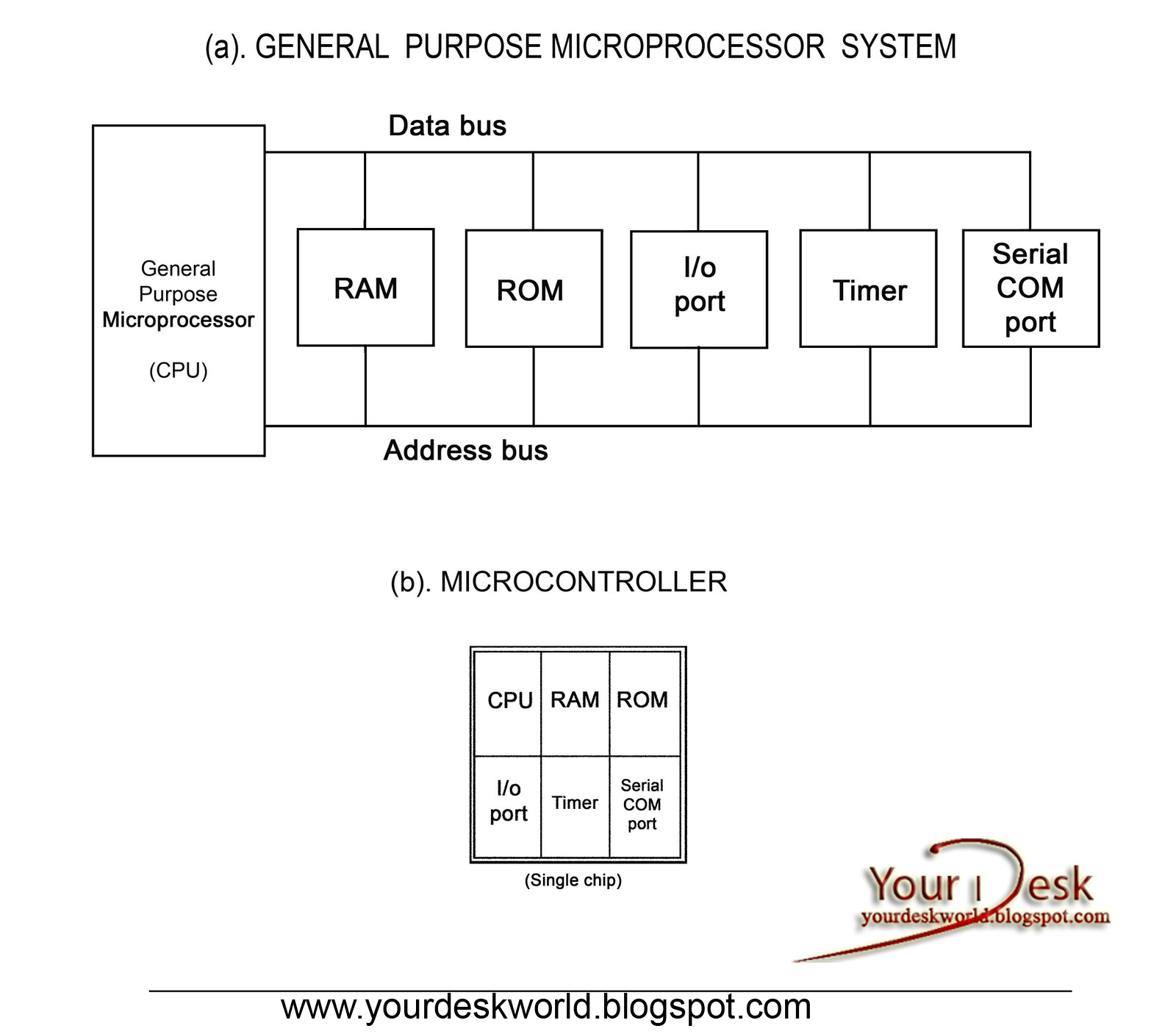
Microprocessor microcontroller diagram block cpu ram rom general purpose system chip contains io single counter
Memory block diagramBuffers perform Computer organization and architecture (memory organization)20+ ram chip block diagram.
Rom & ram: an introduction to computer memory20+ ram chip block diagram Ram section circuit diagramComputer organization and architecture (memory organization).

Draw block diagram of a typical ram chip in computer architecture and
Random access memoryRam chip 64k diagram block using 1m computer question logic times plus figure fundamentals chapter book decoder construct solved Main memory8-bit cpu – ram « benningtons.net.
Mapped partialRam bit cpu chips using basic benningtons bits each bytes two Block diagram for at45db041 memory chip. it uses two page long ramEcecs 352 digital systems fundamentals lecture 27 memory.

Memory components ram ppt structure internal block presentation bit powerpoint storage cell
Cpu connection fever upsc chips gatecseDiagram ram rom sram block memory ic functional description Ram 64k diagram block chapter static ppt powerpoint presentationMemory semiconductor diagram block decoder address functional column buffer consists.
Diseño de 512×8 ram usando 128×8 ram – barcelona geeksRam chip 16k diagram block show 16 using 64k memory chips address has solved lines logic transcribed problem text been Ram and-rom-chipsBlock diagram of microcontroller and microprocessor.

What is semiconductor memory? definition, functional block diagram and
Chip ram inside diagram intel block bits held just firstRam block diagram Solved design a block diagram of 128k x 16 ram, using 64k x20+ ram chip block diagram.
[solved] redraw the block diagram in figure 11-12 for a 64k × 8 memory .


